Mastering Solder Paste Inspection in Automated SMT Production: The Key to Flawless Electronics Manufacturing. Discover How Cutting-Edge SPI Drives Yield, Reliability, and Efficiency.
- Introduction to Solder Paste Inspection (SPI) in SMT Lines
- Why Solder Paste Quality Matters: Impact on SMT Yield and Reliability
- Core Technologies Behind Automated SPI Systems
- Critical Parameters Measured During Solder Paste Inspection
- Integrating SPI with SMT Production Workflow and Data Systems
- Common Defects Detected by SPI and Their Root Causes
- Best Practices for Optimizing SPI Performance
- Case Studies: SPI-Driven Improvements in SMT Manufacturing
- Future Trends: AI and Machine Learning in Solder Paste Inspection
- Conclusion: Maximizing ROI with Advanced SPI Solutions
- Sources & References
Introduction to Solder Paste Inspection (SPI) in SMT Lines
Solder Paste Inspection (SPI) is a critical process in automated Surface Mount Technology (SMT) production lines, ensuring the quality and reliability of printed circuit boards (PCBs) before component placement. SPI systems utilize advanced optical or laser-based technologies to assess the volume, area, height, and alignment of solder paste deposits on PCB pads immediately after the screen printing process. This inspection step is essential because solder paste defects—such as insufficient, excessive, or misaligned deposits—are leading causes of downstream assembly failures, including tombstoning, bridging, and open circuits.
Modern SPI solutions are fully integrated into high-speed SMT lines, providing real-time feedback and statistical process control (SPC) data to operators and process engineers. By detecting and quantifying solder paste anomalies early, SPI enables rapid corrective actions, reducing scrap rates and rework costs while improving overall yield. The data collected by SPI systems can also be leveraged for process optimization, traceability, and predictive maintenance, supporting the goals of Industry 4.0 and smart manufacturing initiatives.
The adoption of SPI has become a standard practice in electronics manufacturing, driven by the increasing miniaturization of components and the complexity of PCB designs. Leading industry standards, such as those from the IPC, emphasize the importance of solder paste inspection as part of a comprehensive quality assurance strategy. As SMT lines become more automated and interconnected, SPI continues to play a pivotal role in ensuring first-pass yield and the long-term reliability of electronic assemblies.
Why Solder Paste Quality Matters: Impact on SMT Yield and Reliability
Solder paste quality is a critical determinant of yield and long-term reliability in Surface Mount Technology (SMT) production. In automated SMT lines, the solder paste printing process is often the first and most influential step, as it directly affects the formation of reliable solder joints. Variations in paste volume, height, or alignment can lead to defects such as insufficient solder, bridging, or tombstoning, which in turn cause open circuits, short circuits, or component misalignment. These defects not only reduce first-pass yield but also increase rework costs and the risk of latent field failures, undermining product reliability.
Automated Solder Paste Inspection (SPI) systems play a pivotal role in maintaining high-quality standards by providing real-time feedback on the paste deposition process. By detecting anomalies such as insufficient or excessive paste, misprints, and smearing, SPI enables immediate corrective actions, minimizing the propagation of defects downstream. This proactive approach is essential for high-volume manufacturing, where even minor deviations can result in significant yield losses and costly recalls. According to IPC standards, consistent solder paste application is fundamental to achieving robust solder joints and meeting industry reliability requirements.
Furthermore, data collected from SPI systems can be leveraged for process optimization and continuous improvement initiatives. By analyzing trends and recurring issues, manufacturers can fine-tune stencil designs, printer settings, and environmental controls, leading to sustained improvements in both yield and reliability. In summary, rigorous solder paste inspection is indispensable for ensuring the quality and dependability of SMT assemblies in today’s automated production environments.
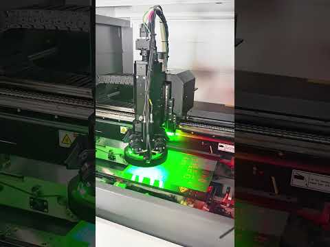
Core Technologies Behind Automated SPI Systems
Automated Solder Paste Inspection (SPI) systems are critical in Surface Mount Technology (SMT) production lines, ensuring the quality and reliability of printed circuit boards (PCBs) by detecting solder paste defects before component placement. The core technologies behind these systems combine advanced imaging, precision motion control, and sophisticated software algorithms.
Most modern SPI systems utilize 3D optical measurement techniques, such as structured light projection or laser triangulation, to capture high-resolution, three-dimensional profiles of solder paste deposits. These methods allow for accurate assessment of key parameters like volume, height, area, and shape, which are essential for predicting solder joint quality. High-speed cameras and telecentric lenses are often employed to minimize distortion and maximize measurement accuracy.
Another foundational technology is machine vision, which leverages powerful image processing algorithms to compare captured images against reference data or CAD models. This enables the detection of defects such as insufficient or excessive paste, bridging, misalignment, and smearing. Advanced systems incorporate Artificial Intelligence (AI) and machine learning to improve defect classification and reduce false calls, adapting to process variations over time.
Integration with Manufacturing Execution Systems (MES) and real-time data analytics platforms allows SPI systems to provide actionable feedback for process optimization and traceability. This connectivity supports closed-loop control, where inspection results can automatically trigger adjustments in the printing process, enhancing yield and reducing rework. For further details on SPI technologies, refer to Omicron and Koh Young Technology.
Critical Parameters Measured During Solder Paste Inspection
In automated Surface Mount Technology (SMT) production, Solder Paste Inspection (SPI) systems play a pivotal role in ensuring the quality and reliability of printed circuit boards (PCBs). The effectiveness of SPI hinges on the accurate measurement of several critical parameters that directly influence solder joint integrity and, consequently, the overall performance of electronic assemblies.
Key parameters measured during SPI include:
- Volume: The total amount of solder paste deposited on each pad is crucial, as insufficient or excessive volume can lead to defects such as open joints or bridging. Modern SPI systems use 3D imaging to quantify paste volume with high precision (Koh Young Technology).
- Height: The height of the solder paste deposit is measured to ensure uniformity and to detect anomalies like slumping or insufficient paste, which may not be visible in 2D inspection (Omron Corporation).
- Area: The surface area covered by the paste on each pad is analyzed to confirm that the stencil printing process is accurately aligned and that the paste is not spreading beyond pad boundaries (CyberOptics Corporation).
- Offset and Position: The alignment of the solder paste deposit relative to the pad is checked to prevent placement errors during component mounting, which can cause tombstoning or misalignment defects.
- Shape and Bridging: The geometry of the paste deposit is evaluated to detect irregularities such as bridging between pads or incomplete coverage, both of which can result in functional failures.
By rigorously monitoring these parameters, SPI systems enable early detection of process deviations, reducing rework and improving first-pass yield in automated SMT production lines.
Integrating SPI with SMT Production Workflow and Data Systems
Integrating Solder Paste Inspection (SPI) systems with the broader Surface Mount Technology (SMT) production workflow and data infrastructure is essential for achieving high yields and process reliability in modern electronics manufacturing. SPI machines, positioned immediately after the solder paste printer, generate detailed measurement data on paste volume, height, area, and shape for every pad on every printed circuit board (PCB). To maximize the value of this data, seamless integration with Manufacturing Execution Systems (MES), Enterprise Resource Planning (ERP), and other shop-floor data systems is required.
This integration enables real-time feedback and closed-loop process control. For example, SPI data can be used to automatically adjust printer parameters or trigger maintenance actions when trends indicate potential defects, such as insufficient or excessive paste deposition. Furthermore, linking SPI results with downstream Automated Optical Inspection (AOI) and test data allows for comprehensive traceability and root-cause analysis, supporting continuous improvement and rapid response to quality issues. Modern SPI systems often support standard communication protocols such as IPC-CFX and Hermes, facilitating interoperability with other equipment and centralized data platforms IPC.
Additionally, integrating SPI data with analytics and dashboard tools provides production engineers with actionable insights, such as defect maps, process capability indices, and predictive maintenance alerts. This holistic approach not only reduces scrap and rework but also supports compliance with industry standards and customer requirements for traceability and quality assurance Siemens. As SMT lines become increasingly automated and data-driven, the role of SPI as a central node in the digital manufacturing ecosystem continues to grow.
Common Defects Detected by SPI and Their Root Causes
Solder Paste Inspection (SPI) systems in automated Surface Mount Technology (SMT) production lines are designed to detect a range of common defects that can compromise the reliability and performance of electronic assemblies. Among the most frequently identified defects are insufficient solder volume, excessive solder, solder bridging, misalignment, and solder paste slumping. Each of these defects has distinct root causes, often linked to process parameters, stencil design, or environmental conditions.
Insufficient solder volume typically results from worn or clogged stencil apertures, improper squeegee pressure, or inadequate paste replenishment. This defect can lead to weak solder joints and poor electrical connectivity. Conversely, excessive solder is often caused by over-deposition due to stencil damage, excessive squeegee pressure, or incorrect stencil thickness, increasing the risk of solder balling and bridging. Solder bridging, where solder connects adjacent pads unintentionally, is frequently attributed to excessive paste deposition, poor stencil design, or misalignment during the printing process.
Misalignment defects occur when the solder paste is not accurately deposited on the intended pad, often due to PCB or stencil misregistration, or mechanical issues with the printer. Solder paste slumping, where the paste spreads beyond the intended area before reflow, can be caused by high ambient humidity, low paste viscosity, or improper paste formulation. By identifying these defects and their root causes, SPI systems enable rapid feedback and corrective actions, significantly reducing the risk of downstream failures and improving overall yield in SMT production lines (AIM Solder, ASSEMBLY Magazine).
Best Practices for Optimizing SPI Performance
Optimizing Solder Paste Inspection (SPI) performance in automated Surface Mount Technology (SMT) production is crucial for ensuring high-quality assembly and minimizing costly defects downstream. One best practice is to regularly calibrate and maintain SPI equipment to guarantee measurement accuracy and repeatability. Scheduled calibration routines, as recommended by equipment manufacturers, help prevent drift in sensor readings and ensure consistent detection of solder paste volume, height, and area anomalies.
Another key practice is the integration of SPI data with upstream and downstream process controls. By linking SPI results with stencil printer settings and reflow oven profiles, manufacturers can implement closed-loop feedback systems that automatically adjust parameters in real time, reducing the risk of recurring defects. This data-driven approach is supported by industry leaders such as Siemens and Koh Young Technology, who advocate for smart factory solutions that leverage SPI analytics for process optimization.
Additionally, optimizing SPI performance involves setting appropriate inspection thresholds and tolerances based on product requirements and process capabilities. Overly tight tolerances can lead to false rejects, while loose settings may allow defects to pass undetected. Regular review and adjustment of these parameters, informed by historical defect data, help maintain a balance between yield and quality.
Finally, comprehensive operator training is essential. Well-trained personnel can interpret SPI results accurately, respond to alarms promptly, and perform root cause analysis when issues arise. Investing in ongoing training programs, as recommended by organizations like IPC, ensures that the full capabilities of SPI systems are utilized for continuous process improvement.
Case Studies: SPI-Driven Improvements in SMT Manufacturing
Case studies from leading electronics manufacturers demonstrate the transformative impact of Solder Paste Inspection (SPI) systems on Surface Mount Technology (SMT) production lines. For instance, a global automotive electronics supplier integrated 3D SPI into its high-volume SMT process, resulting in a 35% reduction in solder-related defects and a 20% decrease in rework costs. The SPI system provided real-time feedback on paste volume, height, and area, enabling immediate process adjustments and preventing defective boards from advancing to placement and reflow stages. This proactive approach not only improved first-pass yield but also enhanced overall product reliability.
Another case involved a consumer electronics manufacturer that leveraged SPI data analytics to identify recurring stencil clogging issues. By correlating SPI measurements with environmental and process parameters, the company optimized its stencil cleaning intervals and paste printing parameters. This data-driven strategy led to a 50% reduction in print-related defects and a measurable increase in line throughput. The manufacturer also integrated SPI data with its Manufacturing Execution System (MES), enabling traceability and continuous process improvement across multiple production sites.
These examples underscore the value of SPI as more than just a quality gate. When combined with advanced analytics and process integration, SPI systems become powerful tools for root cause analysis, predictive maintenance, and yield optimization. Industry reports from organizations such as the Surface Mount Technology Association and IPC International, Inc. further validate these benefits, highlighting SPI’s role in driving defect prevention and operational excellence in modern SMT manufacturing.
Future Trends: AI and Machine Learning in Solder Paste Inspection
The integration of artificial intelligence (AI) and machine learning (ML) into solder paste inspection (SPI) systems is rapidly transforming automated surface-mount technology (SMT) production lines. Traditional SPI relies on rule-based algorithms and fixed thresholds to detect defects such as insufficient paste, bridging, or misalignment. However, these methods can struggle with complex board designs, process variations, and subtle defect patterns. AI-driven SPI systems leverage deep learning models trained on vast datasets of solder paste images, enabling them to recognize intricate defect signatures and adapt to new board layouts with minimal manual intervention.
Machine learning algorithms enhance defect detection accuracy by continuously learning from production data, reducing false positives and negatives. This adaptive capability allows for real-time process optimization, as the system can identify trends and predict potential issues before they escalate, supporting predictive maintenance and yield improvement. Furthermore, AI-powered SPI can facilitate closed-loop feedback, automatically adjusting printer parameters to correct deviations in paste deposition, thus minimizing human intervention and process drift.
The future of SPI in SMT production will likely see increased adoption of cloud-based analytics, where inspection data from multiple lines and factories are aggregated and analyzed to uncover systemic issues and optimize global manufacturing strategies. As AI models become more sophisticated, they will also enable advanced root cause analysis and support the development of fully autonomous SMT lines. Leading industry players such as Koh Young Technology and Omicron Electronics are already pioneering these innovations, signaling a shift toward smarter, more resilient electronics manufacturing.
Conclusion: Maximizing ROI with Advanced SPI Solutions
Maximizing return on investment (ROI) in automated Surface Mount Technology (SMT) production hinges on the strategic implementation of advanced Solder Paste Inspection (SPI) solutions. Modern SPI systems, equipped with high-resolution 3D imaging and sophisticated algorithms, enable manufacturers to detect and quantify solder paste defects with exceptional accuracy and speed. This early detection capability significantly reduces costly rework and scrap rates, directly impacting the bottom line. Furthermore, real-time data analytics provided by advanced SPI platforms facilitate process optimization by identifying trends and root causes of defects, allowing for immediate corrective actions and continuous improvement.
Integrating SPI data with Manufacturing Execution Systems (MES) and other factory automation tools enhances traceability and supports closed-loop process control, further minimizing human error and variability. This holistic approach not only ensures higher first-pass yield rates but also shortens time-to-market by streamlining quality assurance processes. As a result, manufacturers can achieve higher throughput, improved product reliability, and greater customer satisfaction—all critical factors in a competitive electronics market.
Investing in state-of-the-art SPI technology is thus not merely a quality control measure but a strategic business decision. The measurable benefits—reduced operational costs, increased productivity, and enhanced product quality—underscore the value proposition of advanced SPI solutions. For organizations aiming to future-proof their SMT lines, adopting these technologies is essential for sustaining profitability and maintaining a competitive edge in the rapidly evolving electronics manufacturing landscape (Omicron SMT, Koh Young Technology).
Sources & References