Unlocking Unmatched Detail: How High-Resolution Jetting is Transforming Additive Manufacturing. Discover the Breakthroughs Driving Next-Generation Microfabrication.
- Introduction to High-Resolution Jetting Technologies
- Key Principles and Mechanisms of Jetting Processes
- Material Compatibility and Innovations in Jetting Inks
- Comparative Analysis: Jetting vs. Other Additive Manufacturing Methods
- Applications: From Microelectronics to Biomedical Devices
- Challenges in Achieving Ultra-Fine Resolution
- Recent Advances and Emerging Trends
- Quality Control and Metrology for High-Resolution Prints
- Future Outlook: Scaling and Industrial Adoption
- Sources & References
Introduction to High-Resolution Jetting Technologies
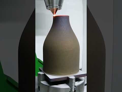
High-resolution jetting technologies represent a transformative approach within additive manufacturing, enabling the precise deposition of materials at microscale and even nanoscale resolutions. Unlike traditional extrusion-based or powder-bed fusion methods, jetting techniques—such as material jetting and binder jetting—utilize printheads to selectively deposit droplets of build material or binding agents, layer by layer, to construct complex geometries with exceptional detail. This capability is particularly advantageous for applications demanding fine feature definition, smooth surface finishes, and multi-material integration, such as in microfluidics, electronics, and biomedical devices.
Recent advancements in printhead design, droplet control, and material formulation have significantly enhanced the achievable resolution, with some systems now capable of producing features below 20 microns. These improvements are driven by innovations in piezoelectric and thermal inkjet technologies, as well as the development of photopolymer and nanoparticle-based inks. The ability to precisely control droplet size, placement, and curing kinetics is critical for minimizing defects and achieving high dimensional accuracy. Furthermore, high-resolution jetting supports the fabrication of functionally graded materials and embedded components, expanding the design freedom for engineers and researchers.
Despite these advantages, challenges remain in terms of material compatibility, print speed, and scalability for industrial production. Ongoing research focuses on expanding the range of printable materials, improving throughput, and integrating real-time process monitoring to ensure consistent quality. As these hurdles are addressed, high-resolution jetting is poised to play a pivotal role in the next generation of additive manufacturing technologies, offering unprecedented capabilities for precision engineering and customized manufacturing National Institute of Standards and Technology, ASTM International.
Key Principles and Mechanisms of Jetting Processes
High-resolution jetting in additive manufacturing (AM) relies on the precise deposition of material droplets to construct complex geometries with fine feature sizes. The core principle involves the controlled ejection of micro- to picoliter-scale droplets from a printhead onto a substrate, where they solidify to form the desired structure. This process is governed by several key mechanisms, including droplet formation, flight, impact, and coalescence, each of which must be finely tuned to achieve high resolution and accuracy.
Droplet formation is typically achieved through thermal, piezoelectric, or electrostatic actuation, each offering distinct advantages in terms of speed, material compatibility, and droplet size control. For instance, piezoelectric printheads can generate highly uniform droplets with diameters as small as 10 microns, enabling the fabrication of intricate microstructures. The rheological properties of the jetting material—such as viscosity and surface tension—play a critical role in ensuring stable jetting and preventing issues like satellite droplet formation or nozzle clogging.
The spatial resolution of jetting processes is further influenced by the precision of the printhead movement and the interaction between deposited droplets. Accurate synchronization between droplet ejection and substrate positioning is essential to minimize placement errors and achieve sharp feature edges. Additionally, the wetting behavior of the substrate affects droplet spreading and coalescence, impacting the final resolution and surface finish of the printed part. Advances in printhead design, material formulation, and process control have collectively enabled high-resolution jetting to produce components with feature sizes below 50 microns, supporting applications in electronics, biomedical devices, and microfluidics (Nature Reviews Materials; National Institute of Standards and Technology).
Material Compatibility and Innovations in Jetting Inks
Material compatibility is a critical factor in achieving high-resolution jetting in additive manufacturing (AM), as the performance and fidelity of printed structures depend heavily on the properties of jetting inks. Traditional jetting processes have primarily relied on photopolymer resins and thermoplastic materials, but recent innovations have expanded the range of compatible materials to include ceramics, metals, and functional composites. These advancements are driven by the need for inks that not only exhibit suitable viscosity and surface tension for precise droplet formation but also maintain stability and reactivity during the jetting and post-processing stages.
One significant innovation is the development of nanoparticle-based inks, which enable the jetting of metals and ceramics with sub-micron resolution. These inks are engineered to prevent agglomeration and sedimentation, ensuring consistent jetting performance and high-density final parts. Additionally, the formulation of multi-material inks allows for the integration of disparate properties—such as electrical conductivity and mechanical strength—within a single printed object, broadening the functional scope of high-resolution AM Nature Reviews Materials.
Another area of progress is the use of reactive and stimuli-responsive inks, which can undergo chemical transformations post-deposition, enabling the fabrication of complex geometries and smart structures. The compatibility of these advanced inks with high-resolution jetting systems is facilitated by ongoing research into rheological modifiers, surfactants, and novel binder chemistries Additive Manufacturing. As a result, the field is moving toward greater material diversity and functionality, paving the way for new applications in electronics, biomedicine, and microfabrication.
Comparative Analysis: Jetting vs. Other Additive Manufacturing Methods
High-resolution jetting stands out among additive manufacturing (AM) techniques for its ability to produce intricate geometries with fine feature sizes, often reaching sub-50 micron resolutions. When compared to other AM methods such as fused deposition modeling (FDM), selective laser sintering (SLS), and stereolithography (SLA), jetting offers unique advantages and trade-offs. Unlike FDM, which extrudes thermoplastic filaments and is limited by nozzle diameter, jetting deposits droplets of material—typically photopolymers or waxes—enabling smoother surfaces and finer details. SLS, while capable of complex geometries and robust mechanical properties, generally produces rougher surfaces and is less suited for applications demanding high visual or dimensional fidelity.
SLA, another high-resolution technique, uses a laser to cure liquid resin layer by layer. While SLA can achieve comparable resolutions to jetting, it is often slower for multi-material or color applications. Jetting, by contrast, can simultaneously deposit multiple materials or colors, making it ideal for prototyping, dental models, and microfluidic devices. However, jetting is typically limited to photopolymer materials, which may not match the mechanical strength or thermal resistance of SLS or FDM parts.
In summary, high-resolution jetting excels in producing detailed, multi-material, and visually accurate parts, but may be constrained by material choices and mechanical properties. The selection of an AM method should thus be guided by the specific requirements of resolution, material, and application context. For further details, see National Institute of Standards and Technology and ASTM International.
Applications: From Microelectronics to Biomedical Devices
High-resolution jetting in additive manufacturing (AM) has emerged as a transformative technology, enabling the precise deposition of materials at the microscale and nanoscale. This capability is particularly impactful in sectors demanding intricate geometries and fine feature sizes, such as microelectronics and biomedical devices. In microelectronics, high-resolution jetting facilitates the fabrication of complex circuit patterns, interconnects, and microelectromechanical systems (MEMS) with sub-10-micron accuracy. This precision supports the miniaturization of electronic components, essential for next-generation devices like flexible displays, sensors, and wearable electronics. For instance, inkjet-based printing techniques have been successfully employed to deposit conductive inks and dielectric materials, streamlining the production of multilayered electronic structures with reduced material waste and lower processing temperatures compared to traditional photolithography National Institute of Standards and Technology.
In the biomedical field, high-resolution jetting enables the creation of patient-specific implants, microfluidic devices, and tissue engineering scaffolds with highly controlled architectures. The technology allows for the precise placement of bioinks, living cells, and growth factors, which is critical for fabricating functional tissues and organ-on-chip systems. This level of control enhances cell viability and function, paving the way for advanced regenerative medicine applications and personalized healthcare solutions National Institute of Biomedical Imaging and Bioengineering. Furthermore, the ability to print at high resolution supports the development of drug delivery devices and diagnostic tools with improved sensitivity and specificity. As high-resolution jetting technologies continue to evolve, their applications are expected to expand, driving innovation across both microelectronics and biomedical domains.
Challenges in Achieving Ultra-Fine Resolution
Achieving ultra-fine resolution in high-resolution jetting for additive manufacturing presents a complex set of challenges that span material science, hardware engineering, and process control. One of the primary obstacles is the precise control of droplet formation and placement. As nozzle diameters decrease to enable finer features, issues such as nozzle clogging, inconsistent droplet size, and satellite droplet formation become more pronounced. These phenomena can degrade print fidelity and limit the minimum achievable feature size. Additionally, the rheological properties of printable materials—such as viscosity and surface tension—must be tightly controlled to ensure reliable jetting at micro- and nano-scales. Many functional materials, including conductive inks or biological suspensions, exhibit non-Newtonian behavior, further complicating jetting dynamics Nature Reviews Materials.
Thermal and mechanical stability of the printhead is another significant concern. High-resolution jetting often requires precise temperature control to maintain material properties and prevent phase separation or premature curing. Moreover, the alignment and synchronization of multi-nozzle arrays become increasingly difficult as feature sizes shrink, leading to potential registration errors and pattern distortions Additive Manufacturing. Post-processing steps, such as curing or sintering, can also induce shrinkage or warping, further impacting the final resolution.
Finally, the trade-off between resolution and throughput remains a persistent challenge. While smaller droplets enable finer features, they also reduce deposition rates, potentially making high-resolution jetting less viable for large-scale or industrial applications. Addressing these challenges requires advances in printhead design, material formulation, and real-time process monitoring National Institute of Standards and Technology (NIST).
Recent Advances and Emerging Trends
Recent advances in high-resolution jetting for additive manufacturing (AM) have been driven by innovations in printhead design, material formulation, and process control. The development of multi-material and multi-nozzle printheads has enabled the deposition of droplets as small as a few picoliters, allowing for feature sizes below 10 microns. This has opened new possibilities for fabricating microfluidic devices, flexible electronics, and biomedical scaffolds with unprecedented precision. Notably, the integration of machine learning algorithms for real-time process monitoring and adaptive control has significantly improved print fidelity and reduced defects, as highlighted by National Institute of Standards and Technology (NIST).
Emerging trends include the use of functional inks containing nanoparticles, living cells, or conductive polymers, which expand the range of applications for high-resolution jetting. Hybrid systems that combine jetting with other AM techniques, such as stereolithography or direct laser writing, are also gaining traction for producing complex, multi-scale structures. Furthermore, advances in in-situ metrology—such as optical coherence tomography and high-speed imaging—are enabling closed-loop feedback systems that further enhance resolution and repeatability, as reported by Lawrence Livermore National Laboratory.
Looking forward, the convergence of novel materials, intelligent process control, and hybrid manufacturing platforms is expected to push the boundaries of high-resolution jetting, making it a cornerstone technology for next-generation microfabrication and personalized medical devices.
Quality Control and Metrology for High-Resolution Prints
Quality control and metrology are critical for ensuring the reliability and performance of high-resolution jetting in additive manufacturing (AM). As jetting technologies achieve feature sizes in the tens of microns or below, even minor deviations in droplet placement, material deposition, or curing can significantly impact the final part’s dimensional accuracy, surface finish, and functional properties. Advanced metrology tools, such as high-resolution optical microscopy, white-light interferometry, and X-ray computed tomography, are increasingly employed to characterize printed features, layer thickness, and internal structures with sub-micron precision. These techniques enable the detection of defects like voids, incomplete curing, or misaligned layers that are often invisible to the naked eye or conventional inspection methods.
In-process monitoring is also gaining traction, leveraging machine vision and real-time feedback systems to detect and correct errors during printing. For example, closed-loop control systems can adjust jetting parameters on-the-fly based on sensor data, reducing the risk of cumulative errors and improving yield. Standards organizations are developing protocols for the measurement and verification of high-resolution AM parts, aiming to harmonize quality benchmarks across the industry. The integration of metrology data with digital twins and process simulation further enhances predictive quality assurance, enabling manufacturers to anticipate and mitigate defects before they manifest in the physical part. As the demand for micro-scale and functionally graded components grows, robust quality control and metrology will remain indispensable for the advancement and industrial adoption of high-resolution jetting technologies in additive manufacturing (National Institute of Standards and Technology, International Organization for Standardization).
Future Outlook: Scaling and Industrial Adoption
The future of high-resolution jetting in additive manufacturing (AM) is poised for significant transformation as the technology matures and scales toward broader industrial adoption. One of the primary challenges lies in maintaining micron-level precision while increasing throughput and build volume, a necessity for cost-effective mass production. Advances in printhead design, multi-material jetting, and real-time process monitoring are expected to address these scalability issues, enabling the fabrication of larger and more complex components without sacrificing resolution or material properties.
Industrial sectors such as electronics, biomedical devices, and microfluidics are particularly well-positioned to benefit from these advancements. For instance, the ability to deposit functional inks with sub-10-micron accuracy opens new avenues for printed circuit boards and lab-on-a-chip devices, where miniaturization and integration are critical. However, widespread adoption will depend on the development of robust, repeatable processes and the standardization of materials and quality assurance protocols. Collaborative efforts between equipment manufacturers, material suppliers, and end-users are essential to establish these standards and accelerate the transition from prototyping to full-scale production.
Looking ahead, the integration of artificial intelligence and machine learning for process optimization, as well as the adoption of digital twins for predictive maintenance and quality control, are likely to further enhance the reliability and efficiency of high-resolution jetting systems. As these innovations mature, high-resolution jetting is expected to become a cornerstone technology in digital manufacturing, driving new business models and applications across diverse industries (ASTM International; Fraunhofer Society).
Sources & References
- National Institute of Standards and Technology
- ASTM International
- Nature Reviews Materials
- National Institute of Biomedical Imaging and Bioengineering
- Lawrence Livermore National Laboratory
- International Organization for Standardization
- Fraunhofer Society