Unlocking Precision and Efficiency: How Vacuum Pick-and-Flip Fixturing Transforms Microelectronic Device Assembly. Discover the Game-Changing Techniques Driving Next-Gen Manufacturing.
- Introduction to Vacuum Pick-and-Flip Fixturing
- Principles and Mechanisms of Operation
- Key Benefits Over Traditional Fixturing Methods
- Applications in Microelectronic Device Assembly
- Design Considerations and Best Practices
- Challenges and Solutions in Implementation
- Case Studies: Real-World Success Stories
- Future Trends and Innovations in Fixturing Technology
- Conclusion: The Impact on Microelectronic Manufacturing
- Sources & References
Introduction to Vacuum Pick-and-Flip Fixturing
Vacuum pick-and-flip fixturing is a critical technique in the assembly of microelectronic devices, enabling the precise handling and orientation of delicate components such as semiconductor dies, microchips, and MEMS structures. This method utilizes controlled vacuum pressure to securely pick up components from a substrate, invert or reorient them as required, and accurately place them onto target locations for further processing or integration. The increasing miniaturization and complexity of microelectronic devices demand high-precision assembly solutions, making vacuum-based fixturing indispensable for achieving reliable alignment and placement at micron or sub-micron scales.
The adoption of vacuum pick-and-flip systems addresses several challenges inherent in microelectronic assembly, including the risk of mechanical damage, contamination, and misalignment that can occur with traditional mechanical gripping methods. By minimizing physical contact and distributing holding forces evenly, vacuum fixturing reduces the likelihood of surface defects and particle generation, which are critical concerns in high-yield manufacturing environments. Furthermore, the ability to automate the pick-and-flip process enhances throughput and repeatability, supporting the stringent quality and productivity requirements of modern semiconductor fabrication lines.
Recent advancements in vacuum tooling design, such as the integration of compliant materials and precision micro-nozzles, have further improved the adaptability and performance of these systems for handling a wide variety of component geometries and sizes. As the industry continues to push the boundaries of device miniaturization and integration, vacuum pick-and-flip fixturing remains a cornerstone technology, supported by ongoing research and development from leading organizations such as SEMI and IEEE.
Principles and Mechanisms of Operation
Vacuum pick-and-flip fixturing is a critical technique in microelectronic device assembly, enabling precise handling and orientation of delicate components such as dies, chips, and microelectromechanical systems (MEMS). The core principle involves the use of controlled vacuum pressure to securely hold a microelectronic device during transfer and manipulation. A vacuum nozzle or collet, typically made from non-abrasive materials to prevent surface damage, creates a pressure differential that gently adheres to the component’s surface. This allows for non-contact gripping, minimizing mechanical stress and contamination risks compared to mechanical tweezers or adhesive-based methods.
The “flip” aspect is essential for processes requiring the reorientation of components, such as die bonding or flip-chip assembly. After picking up the device, the fixturing system—often integrated with robotic arms or precision stages—rotates or inverts the component to the desired orientation. Advanced systems employ programmable motion control and vision alignment to ensure sub-micron placement accuracy, which is vital for high-density interconnects and fine-pitch assemblies. The vacuum is released once the component is correctly positioned, allowing for seamless transfer to the next process step.
Key operational considerations include the design of the vacuum interface to match the component geometry, the regulation of vacuum strength to avoid damage, and the integration with automated assembly lines for high throughput. Recent advancements focus on adaptive fixturing heads and real-time feedback systems to further enhance reliability and yield in microelectronic manufacturing (ASML; Koh Young Technology).
Key Benefits Over Traditional Fixturing Methods
Vacuum pick-and-flip fixturing offers several significant advantages over traditional mechanical fixturing methods in microelectronic device assembly. One of the primary benefits is the reduction of mechanical stress on delicate components. Unlike mechanical grippers or clamps, vacuum-based systems apply uniform pressure, minimizing the risk of physical damage or contamination to sensitive microelectronic devices. This is particularly crucial for handling ultra-thin wafers, fragile die, or components with irregular geometries, where even slight mechanical force can lead to defects or yield loss.
Another key advantage is the improvement in alignment precision and repeatability. Vacuum pick-and-flip tools can be engineered for high positional accuracy, enabling precise placement and orientation of components during assembly. This is essential for advanced packaging techniques, such as flip-chip bonding and wafer-level packaging, where micron-level alignment is required for optimal electrical performance and reliability ASML.
Additionally, vacuum fixturing enhances process flexibility and throughput. The non-contact nature of vacuum handling allows for rapid changeover between different component sizes and shapes without the need for custom mechanical fixtures, reducing downtime and tooling costs. This adaptability is especially valuable in high-mix, low-volume production environments common in advanced microelectronics manufacturing KLA Corporation.
Finally, vacuum pick-and-flip systems can be more easily integrated into automated assembly lines, supporting Industry 4.0 initiatives and enabling real-time process monitoring and control. This integration leads to higher yields, lower defect rates, and improved overall manufacturing efficiency Bosch Global.
Applications in Microelectronic Device Assembly
Vacuum pick-and-flip fixturing has become an essential technique in the assembly of microelectronic devices, particularly where high precision and delicate handling are required. This method is widely applied in the placement and orientation of semiconductor dies, microelectromechanical systems (MEMS), and other miniature components during packaging and integration processes. The vacuum-based approach enables secure, non-contact gripping of fragile parts, minimizing the risk of mechanical damage or contamination that can occur with traditional mechanical tweezers or grippers.
In advanced packaging, such as flip-chip assembly, vacuum pick-and-flip tools are used to accurately pick up dies from a wafer, invert them, and place them onto substrates with micron-level alignment accuracy. This is critical for ensuring reliable electrical connections and optimal device performance. The technique is also instrumental in the assembly of heterogeneous integration platforms, where multiple device types are combined on a single substrate, requiring precise orientation and placement of each component. Additionally, vacuum pick-and-flip fixturing supports high-throughput manufacturing by enabling rapid, automated handling of thousands of devices per hour, which is essential for cost-effective production in the semiconductor industry.
Emerging applications include the assembly of flexible electronics and photonic devices, where the gentle handling afforded by vacuum fixturing is particularly advantageous. As device architectures continue to shrink and become more complex, the role of vacuum pick-and-flip fixturing is expected to expand, supporting innovations in areas such as 3D integration and system-in-package (SiP) technologies (SEMI, imec).
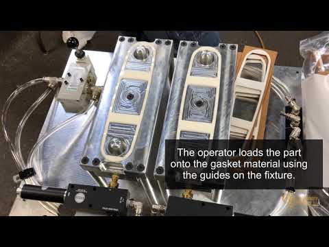
Design Considerations and Best Practices
Designing effective vacuum pick-and-flip fixturing for microelectronic device assembly requires careful attention to both the mechanical and process-specific demands of handling delicate components. Key considerations include the selection of appropriate vacuum tip materials, which must be non-abrasive and chemically inert to prevent contamination or damage to sensitive device surfaces. The geometry of the vacuum tip should be tailored to the component’s size and shape, ensuring secure holding without excessive force that could induce stress or warping.
Alignment accuracy is paramount, as even minor misalignments during the pick-and-flip operation can lead to yield loss or device failure. Incorporating precision-machined alignment features and integrating vision systems for real-time feedback can significantly enhance placement accuracy. Additionally, the fixturing system should minimize particle generation and static buildup, both of which are critical in cleanroom environments. Using antistatic materials and implementing filtered vacuum lines are recommended best practices.
Process flexibility is another important design goal. Modular fixturing platforms that accommodate a range of device sizes and package types can reduce changeover time and improve throughput. Furthermore, ease of maintenance and cleaning should be considered, as residue buildup in vacuum channels can compromise performance over time. Regular inspection protocols and the use of quick-disconnect fittings can facilitate efficient maintenance.
Finally, close collaboration with equipment suppliers and adherence to industry standards, such as those outlined by SEMI and JEDEC, help ensure that fixturing solutions are robust, scalable, and compatible with evolving microelectronic assembly requirements.
Challenges and Solutions in Implementation
Implementing vacuum pick-and-flip fixturing in microelectronic device assembly presents several technical challenges, primarily due to the miniaturization and fragility of components. One major issue is achieving reliable vacuum adhesion without damaging delicate substrates or causing misalignment during the flip process. Variations in surface roughness, material porosity, and device geometry can lead to inconsistent holding forces, risking device slippage or breakage. Additionally, static charge accumulation during vacuum handling can attract particulate contamination, compromising device yield and reliability.
To address these challenges, manufacturers have developed advanced fixture designs with compliant, low-outgassing materials that conform to device surfaces while minimizing mechanical stress. Precision control of vacuum pressure, often through closed-loop feedback systems, ensures consistent and gentle handling across a range of device types. Integration of anti-static materials and ionization systems within the fixturing environment further mitigates contamination risks. Automated vision alignment systems are increasingly employed to correct for any positional errors introduced during the pick-and-flip operation, enhancing placement accuracy and throughput.
Recent research also explores the use of micro-textured vacuum pads and adaptive fixturing platforms that dynamically adjust to varying device geometries, further improving process flexibility and yield. These innovations are supported by industry standards and guidelines, such as those from SEMI and JEDEC, which provide best practices for fixturing and handling in microelectronics assembly. As device dimensions continue to shrink, ongoing development in fixturing technology remains critical to maintaining high assembly quality and throughput.
Case Studies: Real-World Success Stories
The implementation of vacuum pick-and-flip fixturing has led to significant advancements in microelectronic device assembly, as demonstrated by several real-world case studies. For instance, Intel Corporation integrated vacuum-based pick-and-flip systems into their flip-chip assembly lines, resulting in a marked reduction in die misalignment and an increase in throughput. Their adoption of precision vacuum tooling enabled the handling of ultra-thin dies, which are particularly susceptible to mechanical stress, thus improving overall device yield and reliability.
Similarly, Taiwan Semiconductor Manufacturing Company (TSMC) reported enhanced process consistency after deploying automated vacuum pick-and-flip modules in their advanced packaging facilities. The technology allowed for the precise orientation and placement of micro-bumps on high-density interposers, a critical step in 2.5D and 3D integration. TSMC’s case highlights the role of vacuum fixturing in supporting heterogeneous integration and miniaturization trends in the semiconductor industry.
In the field of optoelectronics, OSRAM Opto Semiconductors utilized vacuum pick-and-flip techniques to assemble micro-LED arrays. This approach minimized contamination and mechanical damage, which are crucial for maintaining high optical performance. The company reported a significant decrease in defect rates and an improvement in assembly speed, underscoring the versatility of vacuum fixturing across different microelectronic domains.
These case studies collectively demonstrate that vacuum pick-and-flip fixturing not only enhances precision and yield but also supports the evolving demands of next-generation microelectronic device assembly.
Future Trends and Innovations in Fixturing Technology
The future of vacuum pick-and-flip fixturing in microelectronic device assembly is poised for significant transformation, driven by the increasing demand for miniaturization, higher throughput, and greater assembly precision. One emerging trend is the integration of advanced sensor technologies, such as force and proximity sensors, directly into vacuum tooling. These sensors enable real-time feedback and adaptive control, reducing the risk of device damage and improving placement accuracy, especially for ultra-thin or fragile components. Additionally, the adoption of machine learning algorithms is enabling predictive maintenance and process optimization, allowing fixturing systems to self-adjust parameters based on historical data and in-process monitoring.
Another innovation is the development of modular and reconfigurable vacuum fixtures, which can be rapidly adapted to accommodate a wide variety of device geometries and sizes. This flexibility is crucial for high-mix, low-volume production environments typical in advanced microelectronics manufacturing. Furthermore, the use of novel materials—such as anti-static polymers and ultra-flat ceramics—enhances the cleanliness and reliability of vacuum contact surfaces, addressing contamination and electrostatic discharge concerns.
Automation is also advancing, with collaborative robots (cobots) increasingly being paired with vacuum pick-and-flip systems to streamline assembly lines and reduce human intervention. These advancements are supported by ongoing research and standardization efforts from organizations like SEMI and IEEE, which are shaping the future landscape of microelectronic assembly. As these technologies mature, manufacturers can expect improved yield, reduced cycle times, and enhanced device performance, positioning vacuum pick-and-flip fixturing as a cornerstone of next-generation microelectronic device assembly.
Conclusion: The Impact on Microelectronic Manufacturing
Vacuum pick-and-flip fixturing has emerged as a transformative technique in microelectronic device assembly, significantly enhancing both the precision and efficiency of manufacturing processes. By leveraging controlled vacuum forces, this method enables the secure handling, orientation, and placement of delicate microelectronic components, which are often too small or fragile for traditional mechanical gripping. The adoption of vacuum-based fixturing has led to notable improvements in yield rates and device reliability, as it minimizes the risk of mechanical stress and contamination during assembly operations.
The impact of this technology extends beyond immediate process improvements. Vacuum pick-and-flip systems facilitate the integration of advanced automation, supporting the trend toward high-throughput, scalable manufacturing lines. This is particularly critical as device geometries continue to shrink and the demand for heterogeneous integration grows. The ability to precisely manipulate and align components such as die, MEMS, and optoelectronic elements is essential for next-generation devices, including those used in 5G, IoT, and advanced computing applications. As a result, manufacturers adopting vacuum pick-and-flip fixturing are better positioned to meet stringent quality standards and respond to evolving market requirements.
Looking forward, ongoing innovations in vacuum fixturing—such as adaptive end-effectors and real-time process monitoring—promise to further enhance assembly capabilities. These advancements are expected to drive continued progress in microelectronic manufacturing, supporting the development of more complex, miniaturized, and reliable electronic systems. For further reading on the state-of-the-art in microelectronic assembly, see resources from the SEMI and the IEEE.
Sources & References