Table of Contents
- Executive Summary: 2025 Snapshot & Strategic Insights
- Microwave Optomechanics: Core Principles & Fabrication Breakthroughs
- Market Size, Growth Forecasts & Investment Trends (2025–2029)
- Key Industry Players & Emerging Innovators (e.g. nist.gov, ibm.com, teledyne.com)
- Quantum Applications: Advances in Sensing, Computing, and Secure Communications
- Materials Science: Next-Gen Substrates, Superconductors, and Integration Challenges
- Manufacturing Technologies: Cleanroom Processes, Lithography, and Automation
- Supply Chain Dynamics: Component Availability, Geographic Hubs, and Policy Impact
- Regulatory and Standards Landscape (e.g. ieee.org, asme.org)
- Future Outlook: Disruptive Scenarios, R&D Hotspots, and Strategic Recommendations
- Sources & References
Executive Summary: 2025 Snapshot & Strategic Insights
Microwave optomechanics fabrication in 2025 is characterized by rapid advancements in device integration, precision engineering, and scalable production methods, driven by the increasing demand for quantum technologies and ultrasensitive measurement systems. The field focuses on the manufacture of hybrid devices that couple microwave photons with mechanical resonators, enabling applications in quantum information processing, sensing, and transduction.
Key players such as National Institute of Standards and Technology (NIST), IBM, and Rigetti Computing continue to push the boundaries of superconducting circuit fabrication, incorporating advanced lithography, etching, and deposition techniques to achieve high-quality factor resonators and low-noise microwave circuitry. In 2025, these institutions are scaling up efforts to integrate micromechanical elements onto superconducting chips using silicon-on-insulator (SOI) and piezoelectric substrates, aiming to minimize losses and optimize coupling rates.
Commercial foundries such as GLOBALFOUNDRIES and TSMC have begun offering specialized process modules for MEMS and superconducting components, facilitating the transition of optomechanical devices from academic labs to scalable industrial production. This enables broader accessibility to sophisticated device architectures, including on-chip phononic waveguides and integrated optical-microwave interfaces.
A significant trend in 2025 is the adoption of hybrid integration approaches, where photonic and microwave components are co-fabricated with nanomechanical resonators. For instance, Imperial College London and Spanish National Research Council (CSIC) are demonstrating wafer-scale processes for embedding piezoelectric and optomechanical elements in unified platforms, enhancing device performance and reproducibility.
Looking forward, the next few years will likely see the emergence of turnkey fabrication solutions from both large foundries and specialized quantum hardware startups. The outlook is shaped by ongoing partnerships between academia, government labs, and industry to standardize optomechanical device fabrication, establish robust supply chains for superconducting and piezoelectric materials, and develop automated testing and packaging solutions. This collaborative ecosystem is expected to significantly accelerate commercialization, with microwave optomechanical systems poised to impact quantum computing, secure communications, and high-precision metrology by 2027.
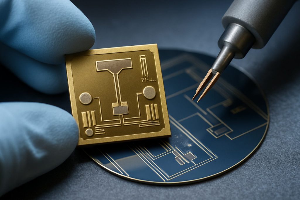
Microwave Optomechanics: Core Principles & Fabrication Breakthroughs
Microwave optomechanics is an interdisciplinary field where mechanical systems are coupled to microwave-frequency electromagnetic fields, enabling exquisite control of mechanical motion through microwave photons. The fabrication of these systems requires advanced techniques that merge expertise from microelectromechanical systems (MEMS), superconducting circuits, and quantum device engineering. As of 2025, the field is witnessing rapid progress in both material science and scalable manufacturing, aiming to improve device performance and integration for quantum computing, sensing, and communication applications.
Recent developments center on reducing mechanical and electromagnetic losses, improving coherence times, and enabling reproducible large-scale integration. Superconducting materials—such as niobium and aluminum—are being deposited using state-of-the-art electron-beam evaporation and sputtering techniques, followed by precision lithography to define microwave resonators and coupling structures. Companies like Oxford Instruments and Janis Research are supplying advanced deposition and cryogenic testing platforms tailored for quantum-grade microwave optomechanical devices.
A significant fabrication breakthrough is the development of on-chip integration schemes, where piezoelectric or optomechanical transducers are co-fabricated with superconducting microwave circuits. National Institute of Standards and Technology (NIST) has demonstrated wafer-scale integration of high-quality silicon and silicon nitride membranes with superconducting aluminum resonators, achieving mechanical quality factors exceeding 107 at low temperatures. These advances enable ultra-sensitive measurements and the transfer of quantum information between microwave and mechanical domains.
Surface and bulk acoustic wave (SAW/BAW) devices, essential for coupling microwaves to mechanical motion, are being refined using advanced etching and wafer-bonding techniques. Cree | Wolfspeed and ROHM Semiconductor are producing high-purity piezoelectric materials, such as gallium nitride (GaN) and lithium niobate, supporting the fabrication of low-loss acoustic resonators and transducers. This is critical for scalable quantum networks and hybrid systems combining photonic and microwave elements.
Looking forward, the field is expected to benefit from investments in 200 mm and 300 mm wafer processing, automated defect inspection, and high-throughput cryogenic testing. Collaborative efforts between device manufacturers and research institutes, such as those supported by Imperial College London Quantum Engineering, are accelerating the transfer of laboratory prototypes to commercial platforms. By 2027, the industry anticipates scalable microwave optomechanical components will be available for integration into quantum processors, distributed sensing arrays, and secure communication nodes, marking a transformative leap in quantum technologies.
Market Size, Growth Forecasts & Investment Trends (2025–2029)
The global landscape for microwave optomechanics fabrication is anticipated to witness robust growth between 2025 and 2029, propelled by increasing demand for quantum technologies, advanced sensing, and high-frequency signal processing. Market participants are intensifying investments in scalable manufacturing capabilities and novel material integration to meet specifications for next-generation quantum devices and hybrid photonic–microwave systems. While quantifying market size is challenging due to the sector’s nascent stage and overlapping applications in quantum computing, telecommunications, and precision measurement, industry activity and public-private investment indicate significant momentum.
Leading developers and suppliers of micro- and nanofabrication equipment, such as Lam Research and Applied Materials, are expanding their process portfolios to support the complex integration of superconducting circuits, high-Q mechanical resonators, and on-chip photonic elements required for microwave optomechanics. These efforts are complemented by foundry initiatives at institutions like NIST and CSEM, which are developing standardized process platforms and offering multi-project wafer runs tailored to quantum and optomechanical device fabrication.
Significant capital is flowing into startups and scaleups focused on quantum hardware and integrated photonics, segments that overlap with microwave optomechanics. For example, Oxford Instruments is channeling R&D into advanced cryogenic and thin-film deposition tools, while Imperial College London Quantum Engineering and QuTech have announced new funding rounds and collaborative projects aimed at bridging lab-scale prototypes and manufacturable optomechanical chipsets.
Looking ahead, market growth from 2025–2029 is expected to be shaped by several drivers:
- Increased public investment in quantum infrastructure (e.g., EU Quantum Flagship, US CHIPS Act) supporting fabrication ecosystem upgrades.
- Expansion of dedicated foundry services for superconducting and photonic quantum technologies by organizations such as imec and Cornell University.
- Rising demand from telecommunications and aerospace sectors for ultra-sensitive microwave–optomechanical sensors and frequency converters.
The sector is likely to see a CAGR in the double digits, with specific growth rates varying by application (quantum computing, metrology, secure communications). The period through 2029 will be characterized by increased industrialization, emergence of contract manufacturing partnerships, and ongoing consolidation among tool and material suppliers. As fabrication technologies mature and fabrication costs decrease, wider adoption of microwave optomechanical modules across quantum and classical domains is expected.
Key Industry Players & Emerging Innovators (e.g. nist.gov, ibm.com, teledyne.com)
The field of microwave optomechanics fabrication is characterized by a blend of established industry leaders and agile emerging innovators, each contributing to advancements in quantum-enabled devices, superconducting circuits, and hybrid photonic-mechanical systems. As of 2025, the sector is witnessing increased collaboration between research institutions and commercial enterprises to accelerate the transition of laboratory-scale demonstrators into scalable, manufacturable technologies.
Among the most prominent players, National Institute of Standards and Technology (NIST) continues to set benchmarks in device miniaturization and integration. NIST’s efforts in the precision fabrication of superconducting microwave resonators and nanomechanical elements are foundational for quantum measurement and information processing platforms. Their recent initiatives focus on improving reproducibility and yield for nano-patterned aluminum and niobium circuits, which are critical for large-scale deployment.
On the industrial front, Teledyne Technologies Incorporated leverages its expertise in microelectromechanical systems (MEMS) and advanced packaging to develop components that satisfy the strict demands of quantum-limited microwave systems. Teledyne’s ongoing work includes the integration of high-purity materials and innovative wafer bonding techniques, enabling reliable coupling between microwave and mechanical modes with minimal loss—an essential requirement for next-generation quantum sensors and transducers.
Meanwhile, IBM is expanding its quantum hardware ecosystem by investing in scalable fabrication processes for superconducting microwave circuits. IBM’s roadmap includes the deployment of foundry-compatible fabrication protocols and robust interconnect technologies, aiming to achieve high coherence and connectivity for quantum processors that integrate mechanical degrees of freedom. IBM’s collaboration with academic partners underscores the importance of hybridizing microwave and mechanical elements to overcome current limitations in scaling and error correction.
Emerging innovators are also shaping the landscape. For example, Black Sesame Technologies and other start-ups are exploring novel materials and multi-layer architectures to unlock new functionalities in microwave optomechanical platforms. Their focus on heterogeneous integration and rapid prototyping accelerates the development cycle, allowing for faster iteration and validation of new device concepts.
Looking ahead, the next few years are expected to see increased standardization efforts and the establishment of dedicated fabrication foundries for quantum and optomechanical circuits. As key players like NIST, Teledyne, and IBM continue to refine their processes and forge partnerships, the industry is poised for significant milestones in manufacturability, reliability, and performance, paving the way for commercialization and deployment in quantum communication, sensing, and computation applications.
Quantum Applications: Advances in Sensing, Computing, and Secure Communications
Microwave optomechanics fabrication is gaining momentum as a critical enabler for quantum technologies in sensing, computing, and secure communications. The field leverages high-precision micro- and nanofabrication techniques to engineer devices that couple mechanical resonators with microwave fields, enabling quantum-level control and readout of mechanical motion. In 2025, the landscape is characterized by rapid refinement in materials, integration platforms, and scalable manufacturing processes, driven by the need for high-coherence, low-loss devices suitable for deployment in quantum systems.
A significant trend is the adoption of superconducting materials, such as niobium and aluminum, in the fabrication of optomechanical circuits. These materials offer ultra-low electrical losses, which are crucial for preserving quantum coherence. For instance, National Institute of Standards and Technology (NIST) continues to pioneer advanced lithography and etching processes to fabricate high-quality superconducting microwave cavities integrated with mechanical elements at the nanoscale. Such platforms are central to quantum transduction and ultra-sensitive detection applications.
Integration with silicon photonics is also advancing. Companies like Intel Corporation are developing hybrid fabrication approaches that combine silicon-based photonic circuits with superconducting microwave components. This integration paves the way for chip-scale quantum microwave-to-optical transducers, essential for linking quantum computers over optical networks. Parallel efforts at IBM focus on scalable wafer-level processing, enabling the mass production of quantum-compatible microwave optomechanical devices.
In terms of device packaging and reliability, Kyocera Corporation and TE Connectivity are working on advanced hermetic packaging and interconnect solutions that maintain cryogenic performance and mechanical stability. These innovations are vital for deploying optomechanical systems in real-world quantum networks and sensors, where environmental isolation and robust connectivity are paramount.
Looking ahead to the next few years, the outlook is shaped by ongoing collaborations between academia, government labs, and industry. Initiatives such as the U.S. Quantum Economic Development Consortium (QED-C) are accelerating the transition from laboratory demonstrations to commercial-scale fabrication, aiming for higher device yields, reproducibility, and integration with emerging quantum processors. As fabrication processes mature, expect to see microwave optomechanics play a foundational role in quantum-enhanced sensing, secure communication links, and the scaling of quantum computing architectures.
Materials Science: Next-Gen Substrates, Superconductors, and Integration Challenges
Microwave optomechanics relies critically on the choice and engineering of materials, as well as the integration of mechanical and microwave elements at micro- and nano-scales. As the field moves through 2025, the materials science community is intensely focused on improving substrate quality, developing next-generation superconductors, and addressing integration complexities to enable scalable and high-coherence microwave optomechanical devices.
A leading trend is the transition toward ultra-low-loss substrates. Silicon-on-insulator (SOI) and high-purity sapphire are increasingly favored for their low dielectric loss and compatibility with superconducting circuitry. Companies such as Wafer World Inc. and Siltronic AG have optimized SOI and high-resistivity silicon wafers for quantum and optomechanical applications. These materials offer atomic-level flatness and reduced parasitic loss, crucial for maintaining coherence in hybrid mechanical-microwave systems.
Superconducting materials remain central to microwave optomechanics, with niobium, niobium nitride, and aluminum thin films being the current mainstays due to their low surface resistance at cryogenic temperatures. However, recent years have seen rapid progress in the fabrication of novel superconductors such as molybdenum-rhenium alloys and tantalum, which demonstrate higher critical temperatures and enhanced resistance to fabrication-induced defects. Oxford Instruments and EV Group have introduced deposition and etching platforms tailored for these advanced materials, offering improved uniformity and process repeatability.
Integration challenges persist, particularly regarding the interface between mechanical resonators (often silicon nitride or piezoelectric materials like aluminum nitride) and superconducting microwave circuits. Achieving strong electromechanical coupling while minimizing cross-talk and parasitic losses demands innovative fabrication approaches. Industry players such as Silterra and TDK Corporation are pioneering MEMS and piezoelectric fabrication processes compatible with superconducting device requirements, including wafer-scale bonding and low-damage etching.
- Outlook (2025–2027): The field is poised to benefit from further substrate quality improvements, especially as wafer-scale integration becomes routine. Adoption of heterogenous integration—combining superconductors, piezoelectrics, and ultra-low-loss substrates on a single platform—is expected to accelerate, with imec and GLOBALFOUNDRIES Inc. investing in advanced packaging and integration solutions. These developments will likely drive advances in device coherence, scaling, and manufacturability, paving the way for practical quantum microwave-optomechanical technologies.
Manufacturing Technologies: Cleanroom Processes, Lithography, and Automation
The fabrication of microwave optomechanical devices in 2025 is evolving rapidly, propelled by advances in cleanroom processes, high-resolution lithography, and increasing automation. These devices, which couple mechanical motion with microwave electromagnetic fields, require extremely precise and contamination-free manufacturing environments to achieve the necessary sensitivity and performance.
Cleanroom facilities have become more advanced, with leading suppliers like Taiyo Nippon Sanso Corporation and Merck KGaA providing ultra-high-purity gases and specialty chemicals vital for thin-film deposition and etching. The push for sub-10 nm feature sizes in superconducting and piezoelectric films, critical for low-loss microwave circuits, is driving adoption of atomic layer deposition (ALD) and molecular beam epitaxy (MBE). Veeco Instruments Inc. continues to offer MBE systems optimized for quantum and microwave device production, while ULVAC, Inc. delivers integrated vacuum solutions for large-scale, reproducible batch fabrication.
Lithography remains a cornerstone, with electron-beam (e-beam) and deep ultraviolet (DUV) photolithography enabling the pattern transfer of sub-micron structures. Companies such as JEOL Ltd. provide high-resolution e-beam lithography systems used in prototyping and small-batch production of optomechanical components such as nanobeams and slot resonators. Meanwhile, ASML Holding N.V. continues to push the boundaries of DUV and EUV photolithography, which are gradually being adapted for specialized microwave and quantum device applications, particularly where scalability is required.
- Automated Wafer Handling: As device complexity increases, automation in wafer handling and process control is crucial for yield and reproducibility. Brooks Automation, Inc. and KLA Corporation deliver solutions for automated wafer transport, inspection, and metrology, helping to minimize human contamination and error.
- Process Integration: Integration of cryogenic-compatible materials and structures is essential for microwave optomechanics. Oxford Instruments plc offers process modules for fabricating superconducting resonators and coupling elements, supporting seamless integration with dilution refrigerators and microwave measurement setups.
Looking ahead, the emphasis in 2025 and beyond will be on scaling up batch fabrication, improving process integration for hybrid quantum-classical systems, and further automating cleanroom workflows. The synergy among established semiconductor equipment manufacturers and emerging quantum technology suppliers is expected to accelerate innovation and lower barriers to commercial deployment of microwave optomechanics.
Supply Chain Dynamics: Component Availability, Geographic Hubs, and Policy Impact
The fabrication of microwave optomechanics systems involves a sophisticated supply chain that encompasses advanced materials, specialized components, and precision equipment. As of 2025, the sector is experiencing both opportunities and challenges driven by global supply chain shifts, emerging geographic hubs, and evolving policy frameworks.
Component availability remains a central concern. Key elements such as high-purity sapphire substrates, superconducting films, and ultra-low-loss dielectric materials are critical for device performance. Suppliers like CRYSTEC GmbH and Cryomech, Inc. provide essential substrates and cryogenic systems, respectively, while Oxford Instruments delivers deposition and etching tools needed for nanofabrication. However, the demand for these specialized materials has outpaced supply in certain regions, leading to longer lead times and heightened competition among research and industry players.
Geographically, the fabrication landscape is shifting. Traditional strongholds in North America and Europe continue to lead, thanks to established research clusters and infrastructure. Notably, the United States hosts several national laboratories and quantum technology hubs, while Europe’s collaborative initiatives, such as those coordinated by CERN, foster cross-border innovation. Meanwhile, East Asia—especially Japan and South Korea—has expanded its role due to robust investment in advanced materials and microfabrication. For instance, Nippon Telegraph and Telephone Corporation (NTT) has accelerated development of optomechanical components and hybrid quantum systems.
Policy impacts are shaping the supply chain in significant ways. The US CHIPS and Science Act and parallel European strategies are targeting domestic industrial capabilities for advanced electronics, including quantum and optomechanical devices. These initiatives aim to reduce reliance on external suppliers, mitigate geopolitical risks, and ensure technology sovereignty. Semiconductor Industry Association has highlighted the importance of such policy support for the resilience of critical component supply chains. At the same time, export regulations and trade restrictions—especially those concerning advanced cryogenic and superconducting technologies—are influencing where and how microwave optomechanics fabrication can be scaled.
Looking forward, the outlook for the supply chain is cautiously optimistic. New investments in fabrication capacity, increased collaboration between suppliers and end-users, and government-backed R&D programs are expected to improve component availability and foster innovation. However, persistent bottlenecks in rare materials and specialized equipment, as well as ongoing geopolitical uncertainties, will continue to require agile supply chain strategies and international cooperation.
Regulatory and Standards Landscape (e.g. ieee.org, asme.org)
The regulatory and standards landscape for microwave optomechanics fabrication has gained heightened attention in 2025, building upon the integration of micro- and nano-fabrication techniques with microwave photonics. As quantum technologies and highly sensitive optomechanical systems become more commercially relevant, industry standards and safety regulations are increasingly critical for ensuring device performance, interoperability, and user safety.
The Institute of Electrical and Electronics Engineers (IEEE) continues to play a leading role in standardizing practices pertinent to microwave and optomechanical device fabrication. Ongoing efforts in 2025 include the expansion of the IEEE 1650 family of standards, originally established for microwave photonic components, now being updated to address hybrid optomechanical systems. The IEEE Standards Association has also initiated working groups to harmonize definitions, measurement procedures, and reliability benchmarks specific to optomechanics, facilitating clearer benchmarks for researchers and manufacturers.
In parallel, the American Society of Mechanical Engineers (ASME) has extended its codes to encompass the mechanical and thermal integrity of micro- and nano-scale optomechanical resonators. The ASME V&V 40 Subcommittee is actively evaluating verification and validation protocols for the simulation of optomechanical components, addressing the unique challenges posed by quantum-limited noise and high-Q mechanical structures.
In 2025, the International Electrotechnical Commission (IEC) has launched new work items under TC 86/SC 86C, focusing on the safety and electromagnetic compatibility (EMC) of integrated photonic and optomechanical modules. This includes guidelines for cleanroom protocols, contamination control, and standards for microwave shielding, which are particularly pertinent to the fabrication environments used by leading industry players.
Manufacturers and research consortia, such as the LFoundry and imec, have begun to align their internal quality assurance procedures with these emerging standards, contributing feedback and data through industry working groups. The adoption of these standards is accelerating collaborative development and transfer of optomechanical fabrication processes across international borders.
Looking ahead, the standards landscape is expected to become more tightly integrated with the needs of quantum information processing, cryogenic operation, and hybrid microwave-optical platforms. Anticipated outcomes include globally harmonized safety protocols and robust certification schemes for optomechanical devices, enabling wider commercial deployment and regulatory compliance in sectors ranging from secure communications to precision sensing.
Future Outlook: Disruptive Scenarios, R&D Hotspots, and Strategic Recommendations
The landscape of microwave optomechanics fabrication is poised for significant transformation in 2025 and beyond, driven by rapid advances in nanofabrication, materials engineering, and quantum technologies. The convergence of these fields is enabling the creation of ever more sophisticated microwave optomechanical systems with potential to disrupt both fundamental research and commercial applications.
- Disruptive Scenarios: The integration of superconducting circuits with high-Q mechanical resonators is expected to yield quantum transducers with unprecedented efficiency. This is crucial for scalable quantum networks and hybrid quantum systems. Pioneering efforts by IBM and Rigetti Computing in superconducting qubit platforms are likely to accelerate the development of compatible optomechanical interfaces. Additionally, the emergence of piezoelectric materials such as lithium niobate on insulator (LNOI) is enabling new device architectures with strong electromechanical coupling, as demonstrated by ams OSRAM and Covestro.
- R&D Hotspots: The ongoing miniaturization of mechanical elements, down to sub-micron and nanometer scales, is a focal point for research teams at NIST and MITRE. They are leveraging electron-beam lithography and advanced etching techniques to achieve high precision and reproducibility. Furthermore, the drive to achieve ultra-low optical and microwave losses has led to collaborative programs between academic labs and leading foundries such as GlobalFoundries and TSMC, aiming to standardize the fabrication of hybrid optomechanical chips for scalable integration.
- Strategic Recommendations: For organizations seeking to establish leadership in this sector, close partnerships with foundries specializing in heterogeneous integration—such as AMD and Intel—will be critical. Investing in custom process development for piezoelectric and superconducting integration is recommended. Companies should also monitor open-access toolsets and process-design kits (PDKs) being developed by LFoundry and Tower Semiconductor, as these will lower barriers to entry and foster ecosystem growth.
Looking ahead, the field will likely experience rapid acceleration as quantum networking and advanced sensing applications move from the laboratory towards commercialization. Stakeholders who invest early in flexible, scalable fabrication technologies, and who engage actively in cross-sector collaborations, will be best positioned to capitalize on disruptive opportunities in microwave optomechanics.
Sources & References
- National Institute of Standards and Technology (NIST)
- IBM
- Rigetti Computing
- Imperial College London
- Spanish National Research Council (CSIC)
- Oxford Instruments
- Janis Research
- Cree | Wolfspeed
- ROHM Semiconductor
- CSEM
- QuTech
- imec
- Cornell University
- Teledyne Technologies Incorporated
- Kyocera Corporation
- QED-C
- Wafer World Inc.
- Siltronic AG
- Oxford Instruments
- EV Group
- Silterra
- Veeco Instruments Inc.
- ULVAC, Inc.
- JEOL Ltd.
- ASML Holding N.V.
- Brooks Automation, Inc.
- KLA Corporation
- Cryomech, Inc.
- CERN
- Semiconductor Industry Association
- Institute of Electrical and Electronics Engineers (IEEE)
- American Society of Mechanical Engineers (ASME)
- ams OSRAM
- Covestro