Fused Deposition Modeling for Functional Electronics Market Report 2025: In-Depth Analysis of Growth Drivers, Technology Innovations, and Global Opportunities. Explore Key Trends, Forecasts, and Strategic Insights for Industry Stakeholders.
- Executive Summary & Market Overview
- Key Technology Trends in Fused Deposition Modeling for Functional Electronics
- Competitive Landscape and Leading Players
- Market Growth Forecasts 2025–2030: CAGR, Revenue, and Volume Analysis
- Regional Market Analysis: North America, Europe, Asia-Pacific, and Rest of World
- Challenges, Risks, and Barriers to Adoption
- Opportunities and Strategic Recommendations
- Future Outlook: Emerging Applications and Long-Term Market Potential
- Sources & References
Executive Summary & Market Overview
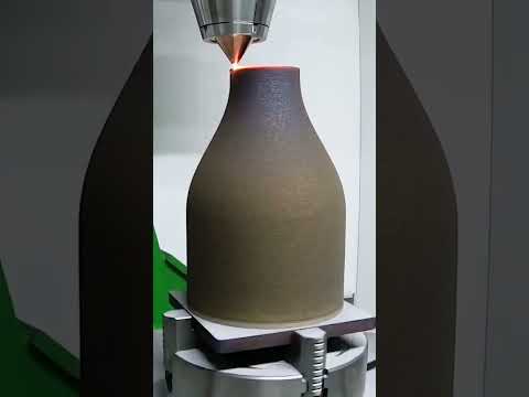
Fused Deposition Modeling (FDM), a subset of additive manufacturing, has rapidly evolved from prototyping to the direct fabrication of functional electronics. In 2025, the global market for FDM in functional electronics is witnessing robust growth, driven by advancements in conductive materials, multi-material printing capabilities, and increasing demand for rapid, customizable electronic device production. FDM enables the layer-by-layer deposition of thermoplastic and composite filaments, now including conductive polymers and metal-infused materials, to create integrated electronic circuits, sensors, and device housings in a single manufacturing process.
The market is characterized by a surge in R&D investments from both established electronics manufacturers and innovative startups. Key players such as Stratasys, 3D Systems, and Nano Dimension are expanding their portfolios to include FDM solutions tailored for functional electronics, targeting applications in consumer electronics, automotive, aerospace, and healthcare sectors. According to IDTechEx, the 3D printed electronics market is projected to surpass $2.5 billion by 2025, with FDM-based approaches accounting for a significant share due to their cost-effectiveness and scalability.
- Technological Advancements: The integration of conductive filaments and hybrid printing heads has enabled the direct printing of functional traces, antennas, and embedded sensors, reducing assembly steps and material waste.
- Customization & Prototyping: FDM’s flexibility supports rapid prototyping and low-volume production of custom electronic devices, accelerating product development cycles for IoT, wearables, and smart devices.
- Market Drivers: The push for miniaturization, lightweighting, and design freedom in electronics manufacturing is fueling adoption, alongside sustainability initiatives that favor additive over subtractive processes.
- Challenges: Despite progress, limitations in resolution, material conductivity, and process repeatability remain barriers to widespread adoption for high-performance electronics.
Geographically, North America and Europe lead in technology adoption, supported by strong innovation ecosystems and government funding for advanced manufacturing. Asia-Pacific is emerging as a high-growth region, propelled by electronics manufacturing hubs and increasing investment in additive manufacturing infrastructure (SmarTech Analysis).
In summary, FDM for functional electronics in 2025 stands at the intersection of material science innovation and digital manufacturing, poised to transform how electronic devices are designed, prototyped, and produced across multiple industries.
Key Technology Trends in Fused Deposition Modeling for Functional Electronics
Fused Deposition Modeling (FDM) is rapidly evolving as a pivotal technology for the fabrication of functional electronics, driven by advances in materials science, hardware innovation, and process integration. In 2025, several key technology trends are shaping the landscape of FDM for functional electronics, enabling new applications and improving device performance.
- Multi-Material Printing: The integration of conductive, dielectric, and structural materials within a single FDM process is becoming increasingly sophisticated. Recent developments allow for the co-extrusion of multiple filaments, including carbon-based and metal-filled polymers, which are essential for printing embedded circuits and sensors. Companies such as Stratasys and Markforged are leading efforts to commercialize multi-material FDM systems tailored for electronics manufacturing.
- Enhanced Conductive Filaments: The market is witnessing the introduction of new conductive thermoplastic filaments with improved electrical properties and printability. These materials, often based on graphene, carbon nanotubes, or silver nanoparticles, enable the direct printing of functional traces, antennas, and interconnects. According to IDTechEx, the demand for advanced conductive materials in additive manufacturing is expected to grow significantly through 2025.
- Integration with Pick-and-Place Automation: Hybrid FDM systems that combine 3D printing with automated pick-and-place of surface-mount devices (SMDs) are gaining traction. This integration streamlines the production of fully functional electronic assemblies, reducing manual intervention and enabling rapid prototyping of complex devices. Nano Dimension and other innovators are developing platforms that merge additive manufacturing with electronics assembly.
- Process Monitoring and Quality Control: Real-time monitoring technologies, such as machine vision and in-situ electrical testing, are being embedded into FDM systems to ensure the reliability and repeatability of printed electronics. These advancements are critical for scaling up production and meeting the stringent quality requirements of industrial and consumer electronics sectors.
- Design Software Advancements: The evolution of CAD and EDA tools tailored for additive electronics is enabling more complex and optimized device architectures. Software from companies like Autodesk now supports the co-design of mechanical and electronic features, facilitating the seamless integration of functional elements within 3D-printed structures.
Collectively, these trends are accelerating the adoption of FDM for functional electronics, opening new possibilities in wearables, IoT devices, and customized electronic components, as highlighted in recent analyses by SmarTech Analysis.
Competitive Landscape and Leading Players
The competitive landscape for Fused Deposition Modeling (FDM) in the functional electronics sector is rapidly evolving, driven by advancements in material science, printer capabilities, and integration with electronic component manufacturing. As of 2025, the market is characterized by a mix of established 3D printing companies expanding into electronics, specialized startups, and collaborations with electronics manufacturers.
Key players include Stratasys, which has leveraged its extensive FDM expertise to develop solutions for embedding conductive materials and sensors directly into 3D-printed parts. Their partnerships with electronics firms have enabled the production of functional prototypes and low-volume end-use electronic devices. 3D Systems is also active in this space, focusing on multi-material FDM processes that allow for the integration of conductive and insulating polymers within a single print job.
Startups such as Nano Dimension are pushing the boundaries with proprietary FDM-based technologies tailored for printed circuit boards (PCBs) and other functional electronic components. Their DragonFly system, for example, enables simultaneous deposition of dielectric and conductive inks, targeting rapid prototyping and on-demand manufacturing for the electronics industry.
Material suppliers play a crucial role in this ecosystem. Companies like DuPont and SABIC are developing advanced thermoplastic filaments with enhanced electrical properties, supporting the functional requirements of embedded electronics. These materials are critical for achieving the necessary conductivity, flexibility, and thermal stability in FDM-printed electronic devices.
Collaborative initiatives are also shaping the competitive landscape. For instance, Autodesk has partnered with hardware manufacturers to optimize design software for FDM-based electronics, streamlining the workflow from digital design to functional prototype. Additionally, research institutions and consortia, such as the America Makes initiative, are fostering innovation through joint R&D projects and standardization efforts.
Overall, the competitive environment is marked by rapid innovation, with companies racing to address challenges such as print resolution, material compatibility, and scalability for mass production. Strategic alliances, intellectual property development, and vertical integration are expected to intensify as the market for FDM in functional electronics matures through 2025 and beyond.
Market Growth Forecasts 2025–2030: CAGR, Revenue, and Volume Analysis
The market for Fused Deposition Modeling (FDM) in functional electronics is poised for robust growth between 2025 and 2030, driven by increasing demand for rapid prototyping, customized electronic components, and advancements in conductive filament technologies. According to projections from MarketsandMarkets, the global 3D printed electronics market—which includes FDM as a key technology—is expected to achieve a compound annual growth rate (CAGR) of approximately 20% during this period. This surge is attributed to the expanding adoption of FDM for producing functional electronic devices such as sensors, antennas, and circuit boards, particularly in sectors like automotive, aerospace, and consumer electronics.
Revenue analysis indicates that the FDM segment within the functional electronics market could surpass $1.2 billion by 2030, up from an estimated $400 million in 2025. This growth is underpinned by the increasing availability of advanced thermoplastic and composite filaments with enhanced electrical properties, enabling the direct printing of complex electronic circuits and components. IDTechEx highlights that the integration of FDM with conductive materials is accelerating the commercialization of printed electronics, with a notable uptick in volume shipments of FDM-printed functional devices expected from 2026 onward.
Volume analysis further supports this optimistic outlook. The annual unit shipments of FDM-printed functional electronic components are projected to grow at a CAGR exceeding 18% through 2030, as reported by SmarTech Analysis. This increase is fueled by the proliferation of desktop and industrial FDM printers capable of processing conductive and dielectric materials, as well as the growing trend of distributed manufacturing and on-demand production in the electronics industry.
Regionally, North America and Europe are expected to maintain leadership in both revenue and volume, owing to strong R&D investments and early adoption by key industry players. However, the Asia-Pacific region is anticipated to exhibit the fastest growth rate, driven by expanding electronics manufacturing hubs and government initiatives supporting additive manufacturing technologies.
In summary, the 2025–2030 period will likely see FDM for functional electronics transition from niche prototyping to mainstream production, with significant gains in market size, shipment volumes, and technological sophistication.
Regional Market Analysis: North America, Europe, Asia-Pacific, and Rest of World
The regional landscape for Fused Deposition Modeling (FDM) in functional electronics is evolving rapidly, with distinct trends and growth drivers across North America, Europe, Asia-Pacific, and the Rest of the World (RoW).
North America remains at the forefront of FDM adoption for functional electronics, propelled by robust R&D investments, a mature additive manufacturing ecosystem, and strong demand from the aerospace, automotive, and consumer electronics sectors. The United States, in particular, benefits from the presence of leading FDM technology providers and a vibrant startup scene focused on printed electronics. Initiatives by organizations such as the National Institute of Standards and Technology (NIST) and collaborations with universities are accelerating the integration of conductive materials and multi-material printing capabilities, enabling the production of complex, functional electronic components.
Europe is characterized by a strong emphasis on sustainability and advanced manufacturing. Countries like Germany, the UK, and the Netherlands are investing in FDM for functional electronics to support the automotive, industrial automation, and medical device industries. The European Union’s focus on digitalization and Industry 4.0, as outlined by the European Commission, is fostering innovation in 3D-printed electronics, with research consortia and public-private partnerships driving the development of new conductive filaments and hybrid manufacturing processes.
Asia-Pacific is witnessing the fastest growth in FDM for functional electronics, fueled by rapid industrialization, government support for advanced manufacturing, and the expansion of consumer electronics production. China, Japan, and South Korea are leading the region, with significant investments in R&D and the establishment of dedicated additive manufacturing centers. According to International Data Corporation (IDC), Asia-Pacific’s additive manufacturing market is expected to outpace global averages, with FDM-based functional electronics playing a key role in prototyping, customized device fabrication, and the integration of smart features into everyday products.
Rest of the World (RoW) markets, including Latin America, the Middle East, and Africa, are at earlier stages of adoption but are showing increasing interest in FDM for functional electronics. Growth is driven by the need for localized manufacturing, cost-effective prototyping, and the gradual expansion of electronics manufacturing capabilities. Initiatives by organizations such as the United Nations Industrial Development Organization (UNIDO) are supporting technology transfer and capacity building in these regions, laying the groundwork for future market expansion.
Challenges, Risks, and Barriers to Adoption
Despite the growing interest in Fused Deposition Modeling (FDM) for functional electronics, several challenges, risks, and barriers continue to impede widespread adoption as of 2025. These obstacles span technical, economic, and regulatory domains, affecting both innovators and end-users.
- Material Limitations: The range of conductive and dielectric materials compatible with FDM remains limited. Most commercially available filaments are optimized for mechanical properties rather than electrical performance. Achieving reliable conductivity, adhesion between layers, and long-term stability in printed circuits is still a significant hurdle. Research into new composite filaments and hybrid materials is ongoing, but commercial availability lags behind demand IDTechEx.
- Resolution and Precision: FDM’s layer-by-layer deposition process inherently limits the resolution and feature size achievable, which is a critical factor for high-density electronic circuits. This restricts the technology’s application to low-frequency, low-complexity devices, and makes it unsuitable for miniaturized or high-performance electronics without significant post-processing SmarTech Analysis.
- Process Integration: Integrating FDM-printed electronics with traditional manufacturing processes is complex. Hybrid approaches often require manual assembly or additional steps, increasing production time and cost. The lack of standardized workflows and interoperability between FDM and pick-and-place or surface-mount technologies further complicates scaling TCT Magazine.
- Reliability and Certification: Printed electronics produced via FDM face challenges in meeting industry reliability standards, especially for mission-critical or safety-related applications. The absence of established testing protocols and certification pathways for 3D-printed electronic components creates uncertainty for manufacturers and end-users UL Solutions.
- Economic Barriers: The cost of specialized conductive filaments and multi-material FDM printers remains high compared to traditional PCB manufacturing, especially at scale. This cost differential is a significant barrier for mass-market adoption, limiting FDM’s use to prototyping, research, and niche applications MarketsandMarkets.
Addressing these challenges will require coordinated advances in materials science, printer hardware, process standardization, and regulatory frameworks to unlock the full potential of FDM for functional electronics in the coming years.
Opportunities and Strategic Recommendations
The market for Fused Deposition Modeling (FDM) in functional electronics is poised for significant growth in 2025, driven by advancements in conductive materials, increasing demand for rapid prototyping, and the push toward miniaturized, customized electronic devices. Key opportunities exist in several high-growth sectors, including wearables, IoT devices, and automotive electronics, where FDM’s ability to integrate conductive traces and components directly into 3D-printed structures offers a competitive edge.
- Material Innovation: The development of new conductive filaments—such as graphene, carbon nanotube, and silver nanoparticle composites—enables the printing of complex circuits and sensors with improved electrical performance. Companies investing in R&D for advanced materials are likely to capture early market share as these filaments become commercially viable (Stratasys, Nano Dimension).
- Integration with Traditional Electronics Manufacturing: Strategic partnerships between FDM technology providers and established electronics manufacturers can accelerate adoption. By combining additive and subtractive processes, manufacturers can produce hybrid devices that leverage the strengths of both approaches, reducing time-to-market and enabling mass customization (Flex, Jabil).
- Prototyping and Low-Volume Production: FDM’s cost-effectiveness for prototyping and small-batch production is particularly attractive for startups and R&D labs. The ability to iterate designs rapidly and produce functional prototypes with embedded electronics shortens development cycles and reduces costs (IDTechEx).
- Customization and On-Demand Manufacturing: The trend toward personalized electronics—such as custom-fit wearables and medical devices—creates a strong use case for FDM. On-demand production reduces inventory costs and enables tailored solutions for niche markets (Gartner).
Strategic recommendations for stakeholders include investing in material science partnerships, developing open-source design libraries for functional electronics, and targeting collaborations with end-users in high-value sectors. Additionally, focusing on regulatory compliance and reliability testing will be crucial for market acceptance, especially in medical and automotive applications. Companies that prioritize ecosystem development—integrating software, hardware, and materials—will be best positioned to capitalize on the expanding opportunities in FDM for functional electronics in 2025.
Future Outlook: Emerging Applications and Long-Term Market Potential
The future outlook for Fused Deposition Modeling (FDM) in the realm of functional electronics is marked by rapid innovation and expanding market potential through 2025 and beyond. As FDM technology matures, its application in producing functional electronic components—such as sensors, antennas, circuit boards, and embedded systems—is gaining significant traction. This shift is driven by the convergence of advanced conductive filaments, multi-material printing capabilities, and the growing demand for rapid prototyping and customized electronics.
Emerging applications are particularly prominent in sectors requiring lightweight, flexible, and geometrically complex electronic devices. For instance, the automotive and aerospace industries are leveraging FDM to integrate sensors and wiring directly into structural components, reducing assembly steps and enabling real-time monitoring functionalities. Similarly, the medical device sector is exploring FDM for patient-specific wearables and diagnostic tools, where embedded electronics can be tailored to individual needs IDTechEx.
The long-term market potential is underpinned by ongoing advancements in printable conductive materials, such as graphene-infused polymers and silver nanoparticle filaments. These materials are expected to enhance the electrical performance and reliability of FDM-printed electronics, making them viable for end-use applications rather than just prototyping. According to SmarTech Analysis, the global market for 3D-printed electronics—including FDM-based solutions—is projected to surpass $2.5 billion by 2030, with a compound annual growth rate (CAGR) exceeding 20% through the latter half of the decade.
Key challenges remain, particularly in achieving fine feature resolution and ensuring consistent electrical properties across printed parts. However, research into hybrid FDM systems—combining extrusion with inkjet or aerosol jet printing—is expected to address these limitations, enabling the fabrication of multilayer circuits and more complex electronic architectures Fraunhofer Society.
In summary, the future of FDM for functional electronics is poised for robust growth, driven by material innovations, hybrid manufacturing approaches, and the increasing need for rapid, on-demand production of smart devices. As these trends accelerate, FDM is set to play a pivotal role in the decentralization and customization of electronics manufacturing.
Sources & References
- Stratasys
- 3D Systems
- Nano Dimension
- IDTechEx
- SmarTech Analysis
- DuPont
- MarketsandMarkets
- National Institute of Standards and Technology (NIST)
- European Commission
- International Data Corporation (IDC)
- SmarTech Analysis
- TCT Magazine
- UL Solutions
- Nano Dimension
- Flex
- Jabil
- Fraunhofer Society